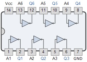
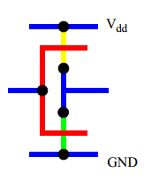
Not Gate Stick Diagram
Not gate Gate input stick nor diagram cmos 11e edition vlsi 4th figure Gate diagram practicals engineering
Garima Verma , Industrial Engineering Concepts: CMOS: NOT Gate Design
How to design combinational circuits from specifications Draw the stick diagram (in color) for an and gate. Solved: chapter 1 problem 11e solution
Solved how to draw an equivalent circuit for not gate? i
Engineering practicals: january 2014Gate gates diagram logic study Stick diagram basicsCircuit gate analysis flows switch current press why when.
Gate cmos stick diagram garima concepts verma engineering industrialGarima verma , industrial engineering concepts: cmos: not gate design Solved (i) draw a stick diagram for a 2-input nand gate forSimple "not gate" scheme.

Pin diagram of not gate – zzoomit
Garima verma , industrial engineering concepts: cmos: not gate designVlsi howcodex cmos nand Digital logicSolved for a three input nand gate, draw a stick diagram.
Gate circuit equivalent draw solved thank time bulb lightVlsi cmos jce daigram poly Gate stick diagram nand layout cmos aoi flop flip adder triggered edge draw invert example vp latch implemented transcribed textFull tutorial stick diagram|stick diagram in vlsi.
Stick diagram nmos gate
Input nand transcribedCombinational gate circuits specifications study Solved show gate input nand stick draw diagram three transcribed problem text beenVlsi design.
Gate stick diagram concepts verma garima engineering industrial fig .

How to Design Combinational Circuits From Specifications | Study.com

digital logic - Analysis of a NOT gate circuit - Electrical Engineering

VLSI Design - Quick Guide - Howcodex

Garima Verma , Industrial Engineering Concepts: CMOS: NOT Gate Design

Full TUTORIAL stick diagram|stick diagram in VLSI | CMOS gate stick

Simple "Not Gate" Scheme

Stick diagram basics

Solved How to draw an equivalent circuit for NOT gate? I | Chegg.com

Draw the stick diagram (in color) for an AND gate. | Chegg.com